Ruijie Networks Released Near-packaged Optics (NPO) & Cold-plate Liquid Cooled Switch
Release time:
2022-10-19
Views:
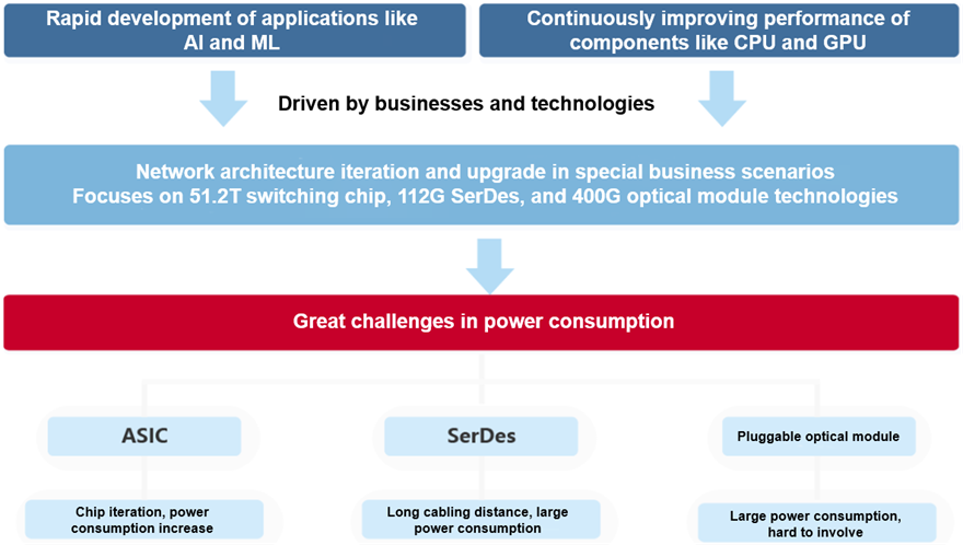
With the development of Internet technologies, data centers are gradually transformed to "computing centers". Applications with large computing power, such as artificial intelligence (AI) and machine learning (ML), are developing rapidly. Diversified businesses, like driverless cars, big data streaming, and interest-based e-commerce, are emerging one after another. Graphics processing unit (GPU) computing clusters, which serve as the basic architecture to support AI, ML, and similar applications, raise higher requirements for network transmission than central processing unit (CPU) common computing clusters. This is the so-called evolution mode of "business-driven network iteration". In this mode, network iteration is performed first in GPU high-performance scenarios to meet the needs of top businesses, and then empowered to common scenarios to give full play to technical values and bonuses.
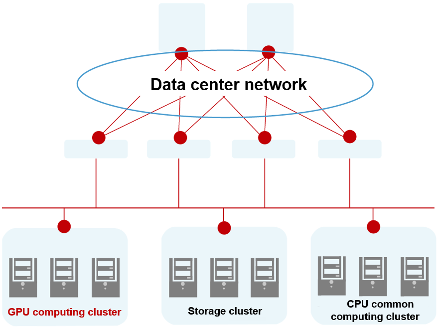
Data Center Network Architecture
In addition to the direct pressure from businesses, the upgrade of data center equipment made to meet functional requirements also invisibly drives the iteration of network devices. For example, for the next-generation H100 GPUs, the required network access bandwidth has now surged to 400 Gbps. For the next-generation CX7 intelligent network interface card (NIC), the network access switch needs to support PAM4-112G serializer-deserializer (SerDes).
Driven by businesses and hardware innovation, it is imperative to upgrade the data center network architecture. For successful iteration, technologies at the three levels of switching chips, SerDes and optical modules must evolve together. It is imaginable that the technological evolution will be hindered by many obstacles, especially the problem of power consumption.
Factors Driving Data Center Network Upgrade and Power Consumption Challenges
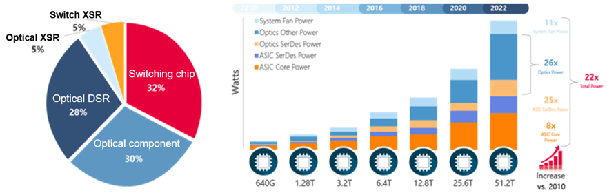
From the aspect of switch chips that determine the performance of switches, although the power consumption of a single bit decreases with the upgrade of switch chips, the total power consumption of switch chips takes a higher proportion in data centers year by year because of the increase of switching bandwidth. Besides, SerDes and optical modules are also major elements of power consumption increase. Statistics show that the total power consumption of a single switch in 2022 is 22 times that in 2010. The power consumption of a SerDes increases by 25 times, and that of an optical module increases by 26 times.
2020 Cisco and/or Its Affiliates (All rights reserved. Cisco Public)
As for the evolution of optical modules, the power consumption of a 10G optical module was less than 1 W in 2007. However, as optical modules are evolved to 40G, 100G, 400G/800G nowadays, and even to 1.6T in the future, the power consumption increases more and more and is approaching 30 W. The power consumption of a switch with full load of 1.6T optical modules would be unimaginable.
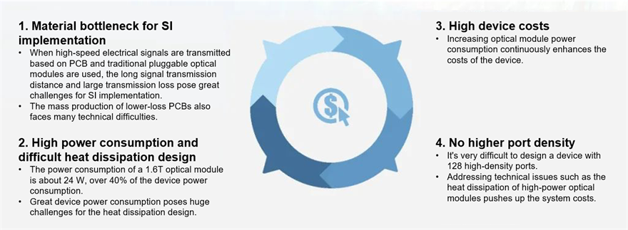
Therefore, the technological evolution of traditional pluggable optical modules is difficult to support the sustainable development of data centers, mainly in the following four aspects:
Bottlenecks in the Technical Development of Traditional Pluggable Optical Modules
1.Material bottleneck for the implementation of signal integrity (SI): When high-speed electrical signals are transmitted based on printed circuit board (PCB) and traditional pluggable optical modules are used, the long signal transmission distance and large transmission loss pose great challenges for SI implementation. The mass production of lower-loss PCBs also face many technical difficulties.
2.Power consumption bottleneck: The power consumption of a device with full load of 1.6T modules is great, posing huge challenges for the heat dissipation design and cabinet power supply.
3.Costs: Greater power consumption accordingly increases the implementation cost of supporting facilities of the device and enhances the initial investment in the network construction.
4.Product design bottleneck: In a system using traditional pluggable optical modules, supporting 128 ports requires a very complex system design. Moreover, technical issues such as the heat dissipation of high-power optical modules push up the system costs.
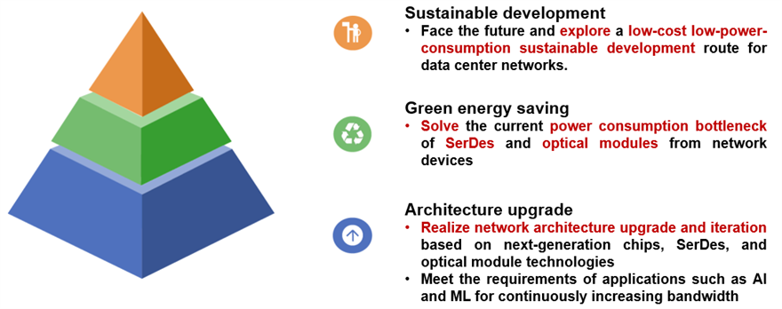
As a result, starting from the power consumption problem of switching chips, SerDes, and optical modules in the iteration of data center network architectures, and aiming to build next-generation, green, energy-saving and sustainable data centers, Ruijie Networks proposes an innovative solution and technical proposal for the sustainable development of data centers based on customers' business scenarios and product practice. The solution is carried out at three layers.
At the bottom layer, the network architecture is upgraded and iterated based on next-generation chips, SerDes, and optical module technologies to meet the requirements of applications such as AI and ML for continuously increasing bandwidth. On the basis of architecture upgrade, the solution tries to solve the current power consumption problem of SerDes and optical modules from network devices. However, the problem occurs not only in this generation and will exist in every generation of network architectures in the future. Therefore, we need to face the future and explore a sustainable development route with low cost and low power consumption for data center networks.
Construction Goals of Next-Generation, Green, Energy-saving and Sustainable Data Centers
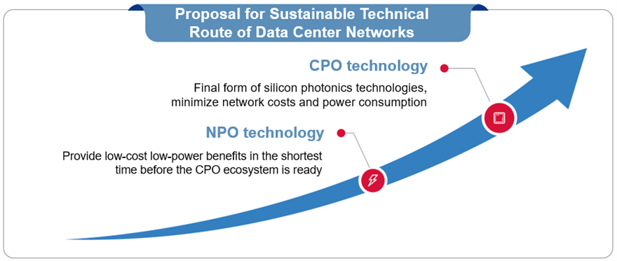
Specifically, the sustainable technical route can be implemented in two development phases of switch silicon photonics technologies: Phase 1: near packaged optics (NPO) technology. This technology provides low-cost low-power benefits in the shortest time before the co-packaged optics (CPO) ecosystem is ready. Phase 2: CPO technology. This is the final form of switch silicon photonics technologies and can minimize network costs and power consumption.
Proposal for Sustainable Technical Route of Data Center Networks
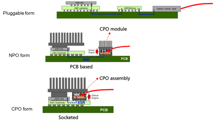
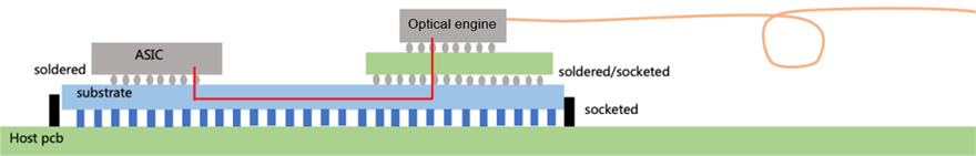
An optical engine conducts the optical/electrical conversion function in a switch network. It is most commonly in pluggable form. With the evolution of technologies, new product forms emerge. The CPO form assembles a switching chip and optical engine in a socketed slot, realizing co-package of the chip and module. The NPO form decouples an optical engine and switching chip, and assembles them on the same system board. Although a photoelectric module exists in both forms, it is packaged in different positions, the corresponding cabling distance varies, and the power consumption is also different.
Overview of Silicon Photonics Technology Forms
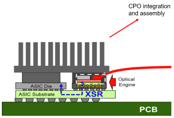
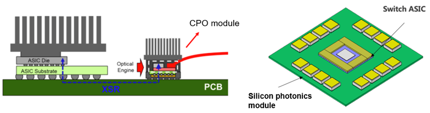
The CPO architecture realizes the form with the highest level of integration based on silicon photonics technologies. It is expected to achieve the optimal cost and power consumption benefits. The core principle of power consumption reduction in the CPO architecture is that the architecture greatly shortens the cabling distance (about 50–70 mm) between the switching chip and the optical engine through co-package. In this way, the CPO architecture reduces the SerDes driver power consumption cost, realizes denser high-speed ports, improves the device bandwidth density, and significantly decreases the power consumption. Due to the higher integration of co-packaged chips and silicon photonics components and the incompleteness of the silicon photonics technology ecosystem, openness is a long-term goal from a commercial perspective.
CPO Architecture
CPO Principle
The NPO architecture of switches can get the fastest benefits in cost and power consumption based on high-integration silicon photonics technologies and open ecosystem. The technical principle of NPO is that through an open optical engine interface, the optical engine is assembled on the same board with the switching chip. The optical engine and chip are decoupled in a standard architecture, which enables flexible selection of the switching chip and NPO module. Although NPO does not have as obvious benefits in power consumption and cost reduction as the CPO architecture, NPO improves openness. As the NPO industry chain becomes increasingly mature, commercial CPO modules are expected to emerge by 2024. As a member of the Optical Internetworking Forum (OIF), Ruijie Networks continuously carries out practical exploration in the field of NPO switches.
NPO Architecture
In November 2021, Ruijie Networks was invited to the Open Compute Project (OCP) Global Summit. At the summit, Ruijie Networks officially launched the 25.6T silicon photonics NPO cold-plate liquid-cooling switch, meeting the requirements of data centers and operators' networks for high reliability.
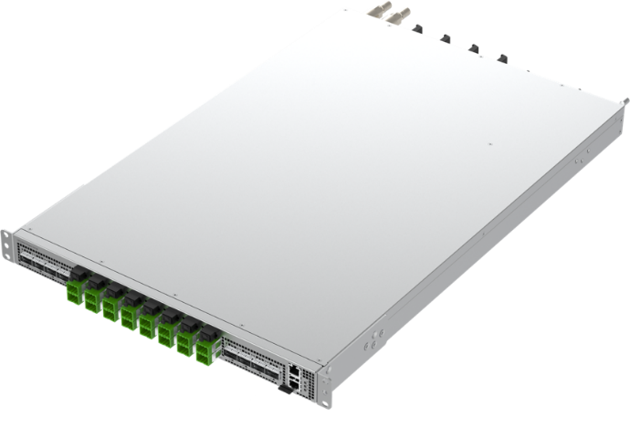
Ruijie 25.6T Silicon Photonics NPO Cold-plate Liquid-cooling Switch
Using the latest 112G SerDes switching chip and 64 connectors, Ruijie 25.6T silicon photonics NPO cold-plate liquid-cooling switch realizes ultra-high-density port design of 64 ports of 400G in 1RU space. The switch consists of 16 × 1.6T (4 × 400G DR4) NPO modules and supports eight external light source (ELS) modules. The wiring distance from the application specific integrated circuit (ASIC) of a PCB to an optical module is shortened by 60%–70%. The high-speed signal quality is greatly improved. The device adopts x86 CPU, fan modules in 3+1 redundancy, and power modules in 1+1 redundancy. The core area uses a cold plate for heat dissipation and non-conductive cooling liquid to eliminate the risk of leakage and short circuit and better support the sustainable development of data center networks.
Ruijie 25.6T Silicon Photonics NPO Cold-plate Liquid-cooling Switch
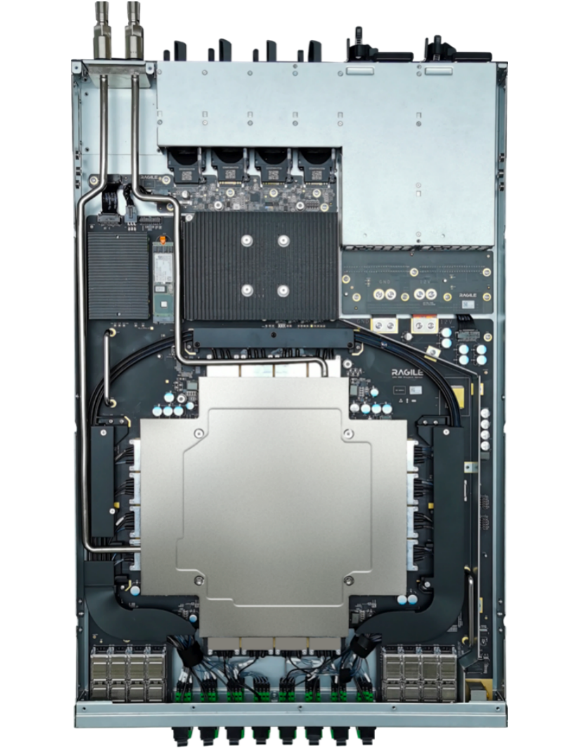
At the optical fiber communication conference and exhibit (OFC) 2022, Ruijie Networks released 51.2T silicon photonics NPO cold-plate liquid-cooling switch based on the 800G NPO prototype of 51.2T switching chip. In 1RU height, the 51.2T switch upgrades NPO modules from 1.6T to 3.2T. The front panel supports 64 × 800G connectors and each connector can be divided into two 400G ports, forward compatible. The number of external light source modules is increased to 16. The blind-mate design is adopted to avoid high-power laser damage to human eyes and protect the safety of O&M personnel. As for heat dissipation, both switching chips and NPO modules support cold plate cooling to realize efficient heat radiation and solve the problem of dense heat flows. Compared with switches with equivalent performance, traditional pluggable optical modules and air cooling solutions, the 51.2T switch greatly reduces the power consumption.
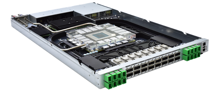
Ruijie 51.2T Silicon Photonics NPO Cold-plate Liquid-cooling Switch
The application scenarios of NPO switches are very wide. The Ruijie 51.2T NPO switch can be applied to the next-generation ultra-large-scale 400G network, and can function as leaf & spine devices to achieve high-speed backbone interconnection. We can achieve commercial release as soon as the end of 2023, helping customers enjoy the values and bonuses of power consumption and cost reduction in the shortest time.
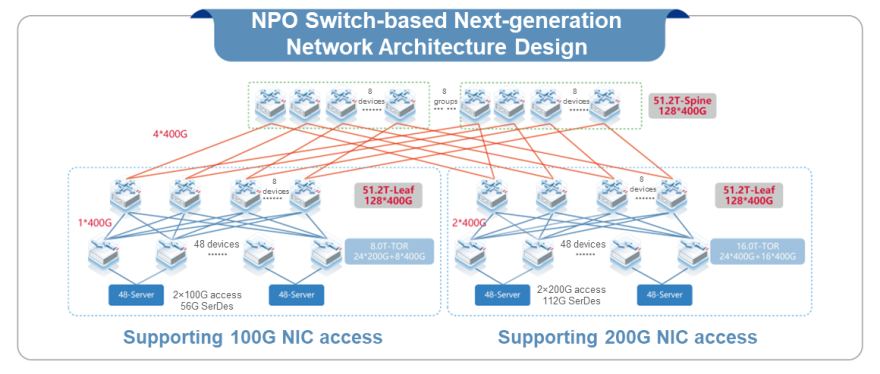
NPO Switch-based Next-generation Network Architecture Design
Ruijie Networks is developing towards the world. As a member of the OIF and Consortium for On-Board Optics (COBO), Ruijie Networks regularly participates in global meetings of silicon photonics-related working groups, and strives to contribute to global technological progress. In the future, Ruijie Networks will go on to practice sustainable development in silicon photonics and develop more products to help customers realize green energy saving.